Synchronous and asynchronous resets
Note: this article discusses resets, but could equally be applied to presets.
This is possibly one of the most widely discussed topics in programmable logic design, but also one of the least understood.
Many FPGA designers are unable to explain why they should choose one or the other and normally just use an asynchronous, active low global reset.
Let’s start with a definition of both types of reset so that we know the difference:
- A synchronous reset will put a flip-flop (or other clocked element) in a predetermined state only when there is an active edge on its clock.
- An asynchronous reset will put a flip-flop (or other clocked element) in a predetermined state whenever it is active, even in the absence of an active clock edge.
Coding these in RTL is straightforward – here are two examples, the first is a flip-flop with an asynchronous, active low reset coded in VHDL:
- process (clk, rst)
- begin
- if (rst ='0') then -- active low async reset
- q <= '0';
- elsif (clk'event and clk='1') then
- q <= d;
- end if;
- end process;
Listing 1: Flip-flop with asynchronous, active low reset
The second is a flip-flop with a synchronous, active high reset coded in SystemVerilog:
- always_ff @(posedge clk) begin: ff_sync
- if (rst == 1) begin
- q <= 0;
- end else begin
- q <= d;
- end
- end : ff_ sync
Listing 2: Flip-flop with synchronous, active high reset
..but before coding a reset, the first thing you should ask is..”do I actually need a reset here?”. Just blindly coding a global reset into your
design will almost certainly lead to a large fanout net which is more difficult to route and that could lead to functional failures
(see explanation below about asynchronous reset deassertion issues).
The fact is that many circuits, especially if they don’t have feedback, can often just use the default, post-configuration state and never need
to be reset. For example, let’s say we have a 128-bit wide data processing pipeline that consists of 128 stages – rather than resetting all 16384
registers, we can just add a single-bit wide shift register of equal depth to that of the data processing pipeline that indicates when the pipeline
output becomes valid. The “valid data” shift register must have a reset – when I hit the reset button on my board, I want to know that the data in the
pipeline is marked invalid and that it won’t be flagged valid again until at least 128 clock cycles later:
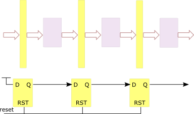
Figure 1: Pipeline with "valid data" flag
Another example is a counter whose only purpose is to divide down a clock, it probably doesn’t need a reset – on the other hand, a counter which is used to count
specific events will almost certainly need a reset to put it back into an initial state.
So which kind of reset should we use? In Xilinx FPGAs, synchronous resets provide a number of advantages:
- The synthesis tools can merge a synchronous reset signal into the logic for the datapath (i.e the LUTs that drive the flip-flop D input). This reduces the fanout on the reset signal and also the number of control sets [insert link to control set article] which in turn improves device packing.
- If you are relying on the tools to infer certain primitives such as DPS48s or BRAMs, this is only possible if you have coded a synchronous reset – these primitives do not support asynchronous resets. Also, the tools cannot merge registers into the DPS48 and BRAM primitives if they have asynchronous reset.
The main disadvantage of a synchronous reset is that a clock must be present for the reset signal to actually have any effect. Designers should pay particular attention to this if they are using gated clocks or on-chip PLLs for frequency synthesis.
Asynchronous resets, by definition, don’t need a clock to be present and it might be necessary to use this kind of reset in certain situations – for example, the Xilinx MMCM and PLL primitives have an asynchronous reset to make sure they go to a known state even if the input clock is not present.
Asynchronous resets however have one major problem – the reset deassertion is not guaranteed to happen at the same clock edge for all synchronous primitives in the design. This means that different parts of the design may exit from reset at different times, there is no control of the reset sequencing.

Figure 2: Asynchronous deassertion problem
Because of the uncertainty as to when the reset will go inactive, some syn chronous primitives will start clocking at edge A whilst others will start clocking at edge B. This problem is only going to get worse as devices get bigger and clock frequencies increase. The solution to this is to synchronize the asynchronous reset to a particular clock domain and guarantee that the reset deassertion is synchronous.
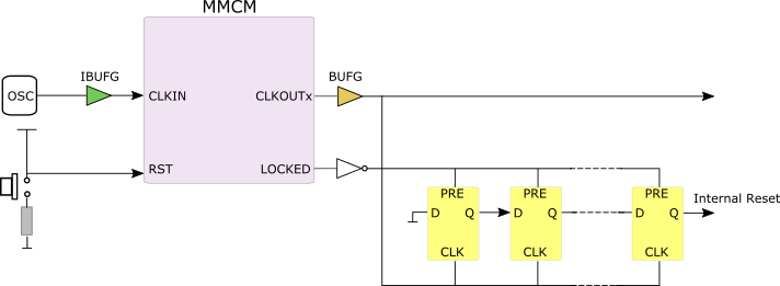
Figure 3: Reset synchronizer circuit
The circuit works like this:
The external asynchronous reset input resets the MMCM causing its LOCK output to go low. The inverted version of the LOCK output asynchronously sets the shift register chain to all 1s –
in this way the internal reset signal is active high. The number of flip-flops in the shift register determines the minimum length of the internal reset pulse. When the MMCM output clock starts up
and LOCK goes high, the shift register begins to shift in the logic ‘0’ until it eventually appears at the output which means that the internal reset has now been deasserted synchronously to the clock.
Note that all of the flip-flops in the shift register are initialised to logic '1' after configuration (bitstream load), this guarantees that an internal reset
pulse will always be generated after FPGA configuration, even if the external reset signal is never activated. This circuit also guarantees that the design will not leave the reset state until the clock
is present and stable.
The circuit could be coded like this:
- signal shiftReg : std_logic_vector(3 downto 0) := (others => '1');
- signal internalReset: std_logic;
- attribute ASYNC_REG : string;
- attribute ASYNC_REG of shiftReg: signal is "TRUE";
- process (clk, locked)
- begin
- if (locked = '0') then
- shiftReg <= (others => '1');
- elsif (clk'event and clk='1') then
- shiftReg <= shiftReg(2 downto 0) & '0';
- end if;
- end process;
- internalReset <= shiftReg(3);
Listing 3: Reset synchronizer circuit code
Note the use of the ASYNC_REG property – see the Vivado Design Suite Properties Reference Guide (UG912) for more information.
In general, one of these synchronizing circuits will be required for each asynchronous clock domain. This will guarantee that the synchronous
elements within each single clock domain exit from reset at the same time (i.e. at the same clock edge). For designs with multiple asynchronous
clock domains, it may be necessary to consider the exit-from-reset sequence of each domain – see the article about clock and reset sequencing for more information.