Clock and reset sequencing is important
A common complaint I hear from users that their FPGA design works "most of the time" but that every so often it boots up in a strange state or just fails to start working. There are multiple possible causes of this kind of problem,
including inadequate power supplies and even silicon issues, but one of the most common causes is a failure to ensure that clocks and resets are correctly sequenced.
There are two main points that need to be checked - the clock start up sequence and the reset/preset release sequence. You need to decide if the order in which clocks (including internally generated clocks) start up is important and then document it in the design specification and verify that the order is respected as
part of the design sign-off and then repeat the process for the resets. Generally speaking, it is more important to consider the reset release sequence rather that the clock start up sequence as most designs
have a synchronized reset for each clock domain.
It is especially important to consider what will happen when we have paths that cross from one domain to another, in these cases we must ensure that a receiving domain is "ready" and will "see" any incoming signals.
In general, it is not important to consider the start up sequence of any clock domains that don't have paths between them - whilst this holds true for the logic inside the FPGA, it may not be true for any off-chip
circuitry driven by the FPGA and designers should also consider this factor as part of their board and system verification.
As an example, consider this case where there are three separate, asynchronous clock domains A, B and C with cross-clock domain signals that pass from domain A to domain C and also from domain B to domain A:
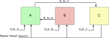
Figure 1: Three clock domain system
We therefore have a requirement that domain A must be ready to receive from domain B before domain starts sending data and we have a similar requirement
between domains A and C.
There are several ways to guarantee that domain B will not transmit to A before it is ready and that domain A
will not transmit to to C before it is ready:
1. Use "ready" flags from A to B and from C to A
The READY flags should be inactive after FPGA configuration and when the clock-domain specific reset is active.
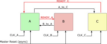
Figure 2: READY flags across clock domains
2. Sequence the resets of all three domains such that the reset release sequence is C -> A -> B
In this case, the resets are effectively in cascade so that C is released first, then A then B. The reset synchronizers (RESET_SYNC_x) use the "Async assertion/sync deassertion" technique.
The master reset causes all reset signals (RESET_x) to immediately go active. RESET_A will not go inactive until after RESET_C is inactive and RESET_B will be held active until RESET_A is inactive.
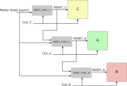
Figure 3: Reset release sequencer