SystemVerilog Clocking Blocks
The clocking block provides a means of specifying the timing of synchronous signals relative to their clock. It defines the timing that the
testbench will use to sample outputs from the DUT and drive inputs towards the DUT. A clocking block can only be declared inside a module, program, interface or checker.
The complete syntax can be found in the SystemVerilog specification (http://standards.ieee.org/getieee/1800/download/1800-2012.pdf) which also contains a
lot of information about their use. Lets skip to a simple example:
- clocking cb_axi @(posedge aclk);
- default input #1ns output #2ns;
- input tready;
- output tvalid;
- output tdata;
- endclocking
Listing 1
The above listing shows the declaration and instance of a clocking block named “cb_axi” (strictly speaking, cb_axi is the clocking identifier).
Note that clocking blocks are implicitly instantiated so there are no separate declaration and instance.
The clock associated with this clocking block is aclk and it uses the rising edge, so the clocking event for this clocking block is @(posedge aclk).
The second line in the clocking block declaration defines the clocking skew times. The input clocking signals declared inside the clocking block
above are all sampled 1ns before the clocking event. The output clocking signals are driven with a delay of 2ns after the clocking event.
Note also that there no widths indicated for the clocking signals – the clocking blocks cannot assign values so widths are not needed.

Figure 1: Input and output skew timing for cb_axi clocking block
So how do we connect the clocking block to the DUT? In a schematic form, it looks like this:
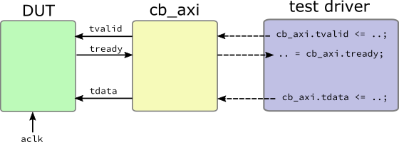
Figure 2: Clocking block and DUT connections
Note how the clocking block inputs are outputs from the DUT and vice-versa.
An (incomplete) example SystemVerilog testbench for the above diagram would look something like this:
- /*-----------------------------
- Signals
- ------------------------------*/
- logic tready;
- logic tvalid;
- logic [31:0] tdata;
- logic aclk;
- /*-----------------------------
- Test driver
- Accesses clkvars, not clocking signals
- ------------------------------*/
- initial begin
- cb_axi.tvalid <= 1;
- cb_axi.tdata <= 32’h01234567;
- do begin
- @(cb_axi); // wait for cb_axi clocking event
- end while (cb_axi.tready == 0);
- end
- /*-----------------------------
- Clocking block
- ------------------------------*/
- clocking cb_axi @(posedge aclk);
- default input #1ns output #2ns;
- input tready;
- output tvalid;
- output tdata;
- endclocking
- /*-----------------------------
- Instantiate DUT
- ------------------------------*/
- axi_periph UUT (
- .ACLK (aclk),
- .TREADY (tready),
- .TVALID (tvalid),
- .TVALID (tdata)
- );
Listing 2
For every clocking signal, there is a corresponding clockvar. A testbench which uses a clocking block should always sample or drive the clockvar, not the corresponding clocking signal. By default, the clockvar name is the same as the corresponding clocking signal. The clockvars are accessed using a dot notation which is made up from the clocking identifier and the clockvar name:
- cb_axi.tvalid <= 1;
Listing 3
Defaults skews
A clocking block like this one that has no definition of skew values is legal and the skews used will be 1step for inputs and zero for the outputs:
- clocking cb_axi @(posedge aclk);
- input tready;
- output tvalid;
- output tdata;
- endclocking
Listing 4
#1step input skew
The 1step is a time unit that denotes a negative time delay before the clocking event such that sampling will occur just before the clocking event. The sampling occurs after all other activity in the current time slot has finished – i.e. in the postponed region of the current time slot.
Setting skew values for individual clocking signals
It is possible to set different skew values for each clocking signal rather use a default value for all of them. In this example the default input skew is #1step and the default output skew is 1 ns, but tvalid and tdata both have their own individual skew values:
- clocking cb_axi @(posedge aclk);
- default input #1step output #1ns;
- input tready;
- output tlast;
- output #2ns tvalid;
- output #4ns tdata;
- endclocking
Listing 5
More complex clocking events
Any valid event expression can be used as the clocking event. For example, a gated clock can be emulated like this:
- clocking cb_gated @(negedge clk iff master_enable);
- default input #1step output #2ns;
- input wrdata;
- output rddata;
- endclocking
Listing 6
The iff statement is a qualifier for the @ event control. The event expression (negedge clk) will only trigger if the expression after iff is true. So the above clocking block will only sample inputs and drive outputs when there is a falling edge on clk and master_enable is true.
Double Data rate (DDR) clock
So far, all of the examples given have explicitly stated if the clocking block uses either the rising edge (posedge) or falling edge (negedge) of its associated clocking event. It may be necessary to specify a double-data rate (DDR) clock where both edges are used. The SystemVeriog specification comes to our rescue here as it contains two examples of how this can be done. The first uses two separate clocking blocks:
- reg j;
- clocking pe @(posedge clk);
- output j;
- endclocking
- clocking ne @(negedge clk);
- output j;
- endclocking
Listing 7
Here, the variable j will have a value that has been assigned by the last clocking block to have been activated by its clocking event. The second example is equivalent to the first, but uses only one clocking block which does not specify posedge or negedge for the clocking event:
- reg j;
- clocking e @(edge clk);
- output j;
- endclocking
Listing 8
Default clocking block
One, and only one, clocking block inside any module, program, interface or checker can be defined as the default clocking clock:
- default clocking cb_gated @(negedge clk iff master_enable);
- default input #1step output #2ns;
- input wrdata;
- output rddata;
- endclocking
Listing 9
When you use the ## delay operator which defines delays in terms of a certain number of clocking events, the clocking events used for the delay will be that defined in the default clocking block.
Using Clocking Blocks With Interfaces
A SystemVerilog interface can contain one or more clocking blocks which can help to simplify the interface timing in simulation. The clocking signals will be sampled or driven relative to the clocking event of the clocking block:
- interface axis (input logic aclk);
- logic [15:0] tdata;
- logic tvalid;
- logic tready;
- // clocking block for AXI Stream master
- clocking cb_axis_mst @(posedge aclk);
- default input #1step output #3ns;
- output tdata;
- output tvalid;
- input tready;
- endclocking
- // clocking block for AXI Stream slave
- clocking cb_axis_slv @(posedge aclk);
- default input #1step output #2ns;
- input tdata;
- input tvalid;
- output tready;
- endclocking
- // AXI stream master modport - for testbench only
- modport tb_axis_mst_mp(clocking cb_axis_mst,
- output tdata,
- output tvalid,
- input tready );
- // AXI stream slave modport - for testbench only
- modport tb_axis_slv_mp(clocking cb_axis_slv,
- input tdata,
- input tvalid,
- output tready );
- // AXI stream master modport - for synthesis
- modport axis_mst_mp(
- output tdata,
- output tvalid,
- input tready );
- // AXI stream slave modport - for synthesis
- modport axis_slv_mp(
- input tdata,
- input tvalid,
- output tready);
- endinterface: axis
Listing 10
Note how there are two clocking blocks needed because we have one for the AXI Streaming master
direction and one for the slave direction. Then there are four modports:
- axis_mst_mp – master, no clocking block, for synthesis
- axis_slv_mp – slave, no clocking block, for synthesis
- tb_axis_mst_mp – master, includes clocking block, only used in testbench
- tb_axis_slv_mp – slave, includes clocking block, only used in testbench
A complete example showing the use of clocking blocks with interfaces and modports can be downloaded.