Locking a bitstream to a single 7-Series device
Tested with Vivado 2015.3
Each Xilinx FPGA has a unique 64bit identification number preprogrammed into it - this is known as the DNA. This ID can be very useful for many
different purposes such as providing a serial number for boards or for keeping a list of authorised
builds - any board
that has an FPGA whose DNA does appear in the list is immediately identified as a being a copy.
The DNA can also be used to provide a degree of active cloning protection - if the device DNA doesn't match the expected value then various
protection measures can be taken.
The complete 64bit DNA can be read via JTAG from the FUSE_DNA register. It is displayed under the properties window in the Vivado Hardware Manager:
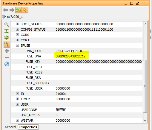
Figure 1: Properties in Vivado
The DNA_PORT primitive provides a way for the internal logic to access 57 bits of the DNA - bits 63:7. The data shift input of the DNA_PORT primitive can be used to
add the other 7 bits so that a comparison can be made with the device's actual DNA and an expected value programmed into the design - that is exactly
what this design does.
The design consists mainly of a tcl script that does the following:
- Reads the FUSE_DNA property from a device.
- Creates an RTL source file (in System Verilog) that compares the expected DNA to the actual DNA read from the device.
- Implements an example design that uses the output of the comparison function to keep a simple LED flasher in reset if the read and expected DNA values don't match.
- Generates a bitstream that has the DNA property in its file name so that it can be easily associated with a particular device.
The example design, SV testbench, instructions and the tcl script are available available from my git hub page.
The example design uses the CFGMCLK clock that comes from the STARTUPE2 primitive - this clock is the output of the ring oscillator used to
generate the master configuration clock. Avoiding the use of an external clock input means the circuit operation cannot be tampered with or held
off by stopping the external clock. It also uses the EOS (end-of-startup) output to enable the comparision circuit to ensure that the DNA check
is done once only after FPGA startup has completed.
The example design simply holds its logic in reset if the actual DNA doesn't match the expected value, but there are an almost infinite
number of possible options, such as:
- Reset the internal MMCMs and PLLs.
- Gate off any or all internal clocks - especially effective if used with clock input pins.
- Drive the GSR or GTS inputs on the STARTUPE2 primitive.
- Enable just a subset of the design's features or a demo-only mode.
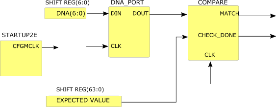
Figure 2: DNA comparison circuit
Security offered by this design
Users should be aware that this design can never be a replacement for a fully secure design that uses features such as AES encryption and authentication. It offers protection against cloning of the design, but it does not protect against reverse engineering or against the use the hardware with another bitstream.